Relevant Links
Project Web Page
Link to Original Paper
Press Contact
Keywords
Memory systems, Silicon photonics, 3D stacking, Memory access protocol
Buzz


![]()
COMPUTING RESEARCH HIGHLIGHT OF THE WEEK [November 11-18, 2011]
New Photonics-Based Access Methods for Main Memory Systems
Multi-core processors demand large amounts of data. Typically, this data is provided by the memory system via electrical pins on a processor package. Unfortunately, the growth in data demands is out-pacing the growth in the number and speed of pins on a package. The impending lack of memory bandwidth will soon choke off processor computations. To address this problem, a significant technology innovation, such as silicon photonics, is required. While a photonic link between processor and memory can provide high bandwidth, expensive photonic components are required on processor and memory chips. The latter is especially problematic because memory chips require low-cost designs.
In a recent paper at ISCA-2011, researchers at the University of Utah and HP Labs introduce a novel memory architecture that enables a photonic link between processor and memory without impacting the cost-sensitive design of memory chips. The memory architecture also enables more autonomy within the memory, thus possibly creating new economic models for the memory industry.
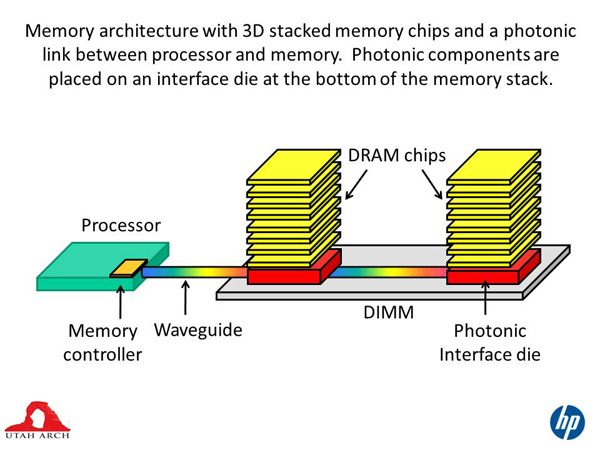
As shown in the figure, 3D stacks of memory chips are employed on a board. At the bottom of the stack is a special interface chip. All photonic components are placed on this interface chip; the optical signal is converted to an electrical signal here and all subsequent intra-stack operations are performed electrically. By leveraging a 3D stack, photonics is used to break the pin barrier while having no negative impact on the design of memory chips. Further, the interface chip can accommodate the complex logic required to perform low-level maintenance and scheduling operations for memory chips. The memory stack is viewed as a black box with a simple interface, allowing memory vendors to add innovative proprietary features. While memory has traditionally been "dumb", the new architecture encourages greater autonomy and smart features within memory stacks, creating new opportunities for innovation.
Researchers:
Aniruddha N. Udipi (University of Utah)
Rajeev Balasubramonian (University of Utah)
Al Davis (University of Utah)
Norman P. Jouppi (HP Labs)
Naveen Muralimanohar (HP Labs)
Institution(s) (that have supported the research):
University of Utah and HP Labs, NSF
‹ Current Highlight | Past Highlights ›
Computing Research Highlight of the Week is a service of the Computing Community Consortium and the Computing Research Association designed to highlight some of the exciting and important recent research results in the computing fields. Each week a new highlight is chosen by CRA and CCC staff and volunteers from submissions from the computing community. Want your research featured? Submit it!.

